Introduction to the ARMv8 Virtualization System
Abstract
ARM processors have taken absolute advantages in mobile devices, but are still developing in the server field. To compete with x86, ARM gradually supports virtualization extensions. This article describes virtualization extensions of ARMv8 processors from dimensions such as the ARM architecture, memory virtualization, interrupt virtualization, and I/O virtualization. This article compares ARM features with x86 features to introduce ARM virtualization extensions.
0. ARMv8 System Architecture
Before getting straight to the point, let's see some basic concepts of the ARMv8 architecture.
ARMv8 supports two execution states: AArch64 and AArch32.
AArch64 (64-bit):
- Provides 31 64-bit general-purpose processors. X30 is the procedure link register.
- Provides a 64-bit program counter (PC), stack pointers (SPs), and exception link registers (ELRs).
- Provides 32 128-bit registers to support SIMD vector and scalar floating-point operations.
- Defines 4 exception levels (EL0 - EL3).
- Supports 64-bit virtual addresses.
- Defines some process state (PSTATE) elements to store processing element (PE) states.
- Uses the ELn suffix to indicate system registers that can be operated at various exception levels.
AArch32 (32-bit):
- Provides 13 32-bit general-purpose registers, one 32-bit PC, SP, and link register (LR).
- Provides a single ELR for abnormal return values in Hyper mode.
- Provides 32 64-bit registers to support SIMD vector and scalar floating-point operations.
- Provides two instruction sets: A32 and T32.
- Supports the ARMv7-A exception model, based on PE modes, and maps this onto the ARMv8 exception model.
- Uses 32-bit virtual addresses.
- Uses a single current program status register (CPSR) to store PE states.
ARM memory model:
- Unaligned memory access generates exceptions.
- Applications are restricted from accessing specified memory areas.
- Virtual addresses in program execution are translated into physical addresses.
- The memory access sequence is controlled.
- Cache and address translation structures are controlled.
- The access to the shared memory between multiple PEs is synchronized.
ARM memory management (see ARM Address Translation):
- The maximum physical memory address width supported by the ARMv8-A architecture is 48 bits, and the page sizes of 4 KB, 16 KB, and 64 KB are supported.
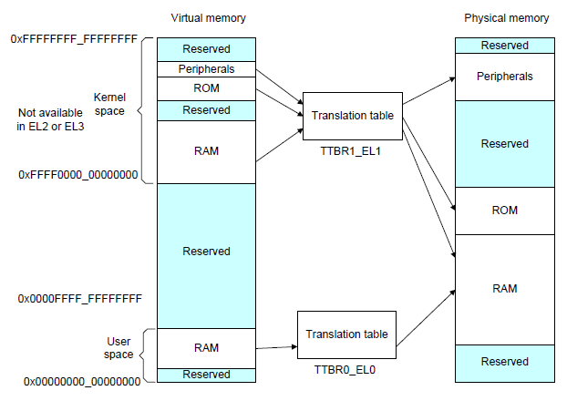
- The virtual memory (VA) management mechanism is used. When the most significant bit (MSB) of a VA is 0, the memory management unit (MMU) uses the translation table of TTBR0 for translation. When the MSB of a VA is 1, the MMU uses the translation table of TTBR1 for translation.
- EL2 and EL3 have TTBR0 but do not have TTBR1, which means that only virtual address space within the 0x0 to 0x0000FFFF_FFFFFFFF range can be used under EL2 and EL3.
-------------------------------------------------------------------------
AArch64 Linux memory layout with 4KB pages + 4 levels::
  Start			End			Size		Use
  0000000000000000	0000ffffffffffff	 256TB		user
  ffff000000000000	ffffffffffffffff	 256TB		kernel
-------------------------------------------------------------------------
Now, we have a preliminary understanding of ARMv8-A. Let's see how ARMv8 supports virtualization from the following dimensions.
1. ARMv8 Virtualization Extension Overview
To support virtualization extensions, ARM introduces the concept of exception level to the CPU running level. The following figure shows the exception levels of AArch64.

- EL0: running level of user-mode programs. Applications in the guest also run at this level.
- EL1: kernel running level. The guest kernel also runs at this level.
- EL2: hypervisor running level. During the running process, the guest triggers privileged instructions and enters EL2 to hand over the control right to the hypervisor.
- EL3: monitor mode. When the CPU switches between the secure world and normal world, it enters EL3 first and then switches between the worlds.
Note: When virtualization extension of the CPU is disabled, software runs at EL0 and EL1. In this case, EL1 has the permission to access all hardware.
ARM exceptions are classified into synchronous exceptions and asynchronous exceptions.
- Synchronous exceptions: undefined exceptions, unaligned exceptions, trap execution exceptions, and system call exceptions. For example, SVC, HVC, and SMC. SVC is used by applications to apply for privileged OS operations or access system resources. HVC is used to apply for hypervisor services. SMC is used to apply for firmware services.
- Asynchronous exceptions: interrupts
Different from ARMv8, x86 introduces the concepts of root mode and non-root mode and a set of special VMX instructions to support CPU virtualization.
The non-root mode is the execution environment of the guest CPU, and the root mode is the execution environment of the host CPU.
The root/non-root mode and CPU privilege levels are independent concepts. They are orthogonal. That is, the user mode (Ring 3) and kernel mode (Ring 0) in non-root mode are the same as those in root mode.
However, ARM CPUs support virtualization mode switching by switching between different ELs.
Nevertheless, ARM and x86 have something in common: If sensitive instructions are executed in virtualization mode, ARM and x86 exit to EL2 and the root mode, respectively.
In addition, x86 implements a data structure called VMCS in memory to better support the root and non-root modes. It is used to store and restore the register information during the switching between the root and none-root modes. The VMX instruction set is used to operate the VMCS data structure.
However, on RISC-based ARM processors, there is no similar implementation. Instead, the hypervisor determines which information needs to be saved and restored, which is more flexible to some extent (see Reference 1).
To optimize the virtualization context switching overhead caused by multiple ELs, ARMv8 introduces the virtual host extension (VHE) feature. See Reference 2. The principle is to directly run the host kernel on EL2. To implement this, the HCR_EL2 register is introduced to control this feature. The advantage of VHE is that two exception level switchovers are reduced, and only some host contexts need to be saved and restored, reducing virtualization overheads and thereby improving the performance.
2. Memory Virtualization
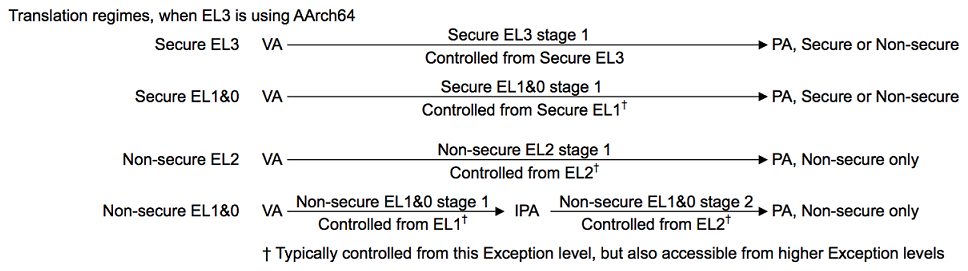
On ARMv8-A, each translation regime may include one or two stages.
Each exception level has its own address translation mechanism and uses different page table base address registers. Address translation can be allocated to stages.
Most ELs include one stage of address translation, and non-secure EL1 and EL0 includes two stages of address translation.
Each stage has its own series of translation tables, and each stage can be enabled or disabled separately. In each stage, the input address (IA) is translated into the output address (OA) (see Reference 3).
Therefore, in virtualization scenarios, the solutions on ARM and x86 are similar. Both of them use two-stage address translation to implement address translation from the guest physical address (GPA) to the host physical address (HPA).
The virtual machine (VM) runs at none-secure EL1 and EL0. When a process in the VM accesses the guest virtual address (GVA), the MMU translates the GVA into an intermediate physical address (IPA), which is a GPA. This is the stage-1 address translation. Then, the MMU translates the IPA into the HPA again. This is the stage-2 address translation.
There are different address spaces at different ELs. How is the translation of different address spaces controlled?
ARMv8-A uses a translation control register (TCR) to control address translation. For example, for EL1 and EL0, because the VA has two independent mapping spaces (user space and kernel space) in this running mode, two page tables are required to complete address translation. The base addresses of the two page tables are stored in TTBR0_EL1 and TTBR1_EL1 respectively.
For each address translation stage:
- A system control register bit is used to enable address translation in this stage.
- A system control register bit is used to determine the endian mode used during translation.
- A translation control register is used to control the address translation process in the entire stage.
- If a VA can be mapped to two subranges in an address translation stage, different TTBRs need to be provided for each VA subrange.
For details, you can sort out KVM-related code. The code is mainly implemented in arch/arm/mm/mmu.c.
3. I/O Virtualization
The purpose of device passthrough is to enable VMs to directly access physical devices, improving I/O performance.
x86 uses the VT-d technology to implement device passthrough based on the VFIO driver and Intel IOMMU.
What are the differences and improvements on ARMv8-A to support device passthrough?
Similar to x86, the key to device passthrough on ARM is to solve the problems of DMA remapping and interrupt delivery of passthrough devices.
However, ARMv8-A uses SMMUv3.1 to process DMA remapping and the GICv3 interrupt controller to implement interrupt delivery. SMMUv3 and GICv3 take many virtualization implementations into consideration during design, and make improvements for virtualization scenarios.
First, let's look at the implementation of SMMUv3.1 in ARMv8-A and its benefits for ARM device passthrough (see Reference 4).
SMMUv3 must support the following features:
- Two-stage address translation, which is similar to the two-stage address translation supported by the MMU in the memory virtualization scenario.
Address translation in the first stage is used for isolation between software entities or DMA isolation in the OS.
Address translation in the second stage is used for DMA remapping. That is, the DMA initiated by the guest is mapped to the guest address space. - 16-bit address space IDs (ASIDs)
- 16-bit virtual machine IDs (VMIDs)
- SMMU page table sharing. Software can select a created shared SMMU page table or create a private SMMU page table.
- 49-bit virtual addresses (matching ARMv8-A's 2×48-bit translation table input sizes). SMMUv3.1 supports 52-bit VAs, IPAs, and PAs.
SMMUv3 also supports the following features (optional):
- Both stage 1 and stage 2 support the AArch32 large page address extension (LPAE) and AArch64 address translation table formats (for compatibility).
- Secure stream (secure DMA stream transfer)
- SMMU TLB invalidation broadcast
- The Hardware Translation Table Update (HTTU) hardware is used to automatically update the Access/Dirty flag of the page table.
- PCIe ATS and PRI (The PRI feature is very powerful and will be described later.)
- 16 KB or 64 KB page tables
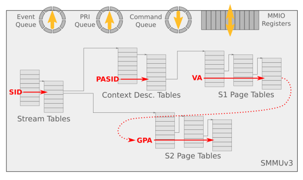
As we know, a platform can have multiple SMMU devices, and each SMMU device may be connected to multiple endpoints.
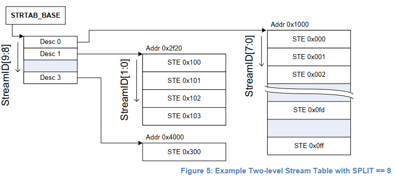
Multiple devices may not reuse the same page table and need to be distinguished. The SMMU uses the stream ID to distinguish the devices.
It searches for the corresponding stream table entry (STE) in the stream table based on the stream ID.
x86 has a similar distinguishing mechanism. The difference is that x86 uses request IDs. By default, a request ID is a B/D/F combination allocated to a PCI device.
According to the SMMUv3 specifications, the stream ID of a PCI device is the request ID of the PCI device.
In addition, a device may be used by multiple processes, which have multiple page tables. The device needs to distinguish the page tables. The SMMU uses substream IDs to distinguish the page tables.
The concept of substream ID is equivalent to that of PCIe process address space ID (PASID).
The maximum width of a substream ID is 20 bits, which is the same as that of the PCIe PASID.
What's in an STE? According to the specifications:
- An STE contains a pointer pointing to the stage-2 address translation table and a pointer pointing to the context descriptor (CD).
- A CD is a data structure in a specific format. It contains the base address pointer to the stage-1 address translation table.
Theoretically, multiple devices can be associated with one VM. Therefore, multiple STEs can share one stage-2 translation table.
Similarly, multiple devices (streams) can share the same stage-1 configuration. Therefore, multiple STEs can share the same CD.
A stream table is stored in memory and is created by the driver when the SMMU device is initialized.
The stream table supports two formats: linear stream table and two-level stream table.
A linear stream table linearly expands the entire stream table into an array in memory, which facilitates indexing. However, continuous memory space is wasted when there are a small number of peripherals on the platform.
A two-level stream table is split into two levels for indexing, which saves memory.
When two-stage address translation of the SMMU is enabled, the VA sent by the device DMA request is translated into the IPA in stage 1, and the IPA is used as the input of stage 2. In stage 2, the IPA output in stage 1 is translated again to obtain the PA. In this way, the DMA request correctly accesses the address space to be operated by the guest.
In stage-1 address translation, the hardware indexes the STE based on the stream ID, and then indexes the CD based on the substream ID. The CD contains the page table base address information, per-stream configuration information, and ASID required for stage-1 address translation (translating the GVA/IOVA of the process into the IPA). In stage-1 translation, multiple CDs correspond to multiple stage-1 address translations, and the matching stage-1 address translation page table is determined by the substream ID. Therefore, stage-1 address translation is actually a mapping process from the request ID/PASID to GPA.
Note: The substream ID is available only when stage-1 address translation is enabled. Otherwise, the DMA request is discarded.
In stage-2 address translation, the STE contains the page table base address (IPA -> HPA) and VMID information for stage-2 address translation. If multiple devices are passed through to the same VM, they share the same stage-2 address translation page table (see Reference 5).
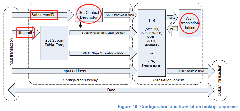
Note that the CD contains an ASID, and the STE contains a VMID. The ASID and VMID are used as TLB tags to accelerate address translation.
The system software interacts with the SMMU through the command queue and event queue. The two queues are cyclic queues.
System software places commands in the command queue, and the SMMU reads the commands from the queue and executes the commands. In addition, the device reports an event when a DMA transfer or configuration error occurs.
These events are stored in the event queue. System software reads events from the event queue in a timely manner to prevent queue overflow.
The aim of two-stage address translation of the SMMU is to support the shared virtual memory (SVM) feature in virtualization scenarios.
The SVM feature allows each process on a VM to independently access a passthrough device that is directly associated to the VM and initiate DMA requests to the device in the process's own address space.
The SVM enables each process in the VM to independently use a passthrough device, which can reduce application programming complexity and improve security.
To implement SVM in virtualization scenarios, QEMU needs to simulate a vSMMU (or vIOMMU).
When an internal process of a VM needs to access a passthrough device, the VM invokes the guest driver to create a PASID table (this table is in the guest in virtualization scenarios).
The PASID is used as an identifier of the process address space in the VM. When a device initiates a DMA request, a PASID prefix is carried with the request. In this way, the SMMU can distinguish devices.
When a PASID table is created, the vSMMU is accessed. In this way, the guest transfers the PASID table address (GPA) to QEMU.
Then, QEMU sends the table information to the SMMU through the IOCTL call (VFIO_DEVICE_BIND_TASK) of VFIO. In this way, the SMMU obtains the shadow information of the PASID table of the guest internal process and can create a stage-1 address translation table.
In short, in two-stage address translation, the DMA request is processed as follows in the guest:
Step 1: The guest driver initiates a DMA request that contains a GVA + PASID prefix.
Step 2: The DMA request reaches the SMMU. The SMMU extracts the request ID from the DMA request to identify the device that sends the request, and then searches the stream table for the corresponding STE.
Step 3: The SMMU finds the CD in the STE, and then uses the PASID to index the CD for the corresponding stage-1 page table.
Step 4: The IOMMU performs stage-1 page table walk, translates the GVA into GPA (IPA), and uses the GPA (IPA) as the input of stage 2.
Step 5: The IOMMU performs stage-2 page table walk to translate the GPA into HPA.
SMMUv3 is similar to Intel IOMMU in design and functions. However, ARM SMMUv3 has two interesting improvements: One is to support the Page Request Interface (PRI), which is a further improvement of the ATS. If the device supports the PRI feature, when the device sends a DMA request, an I/O page fault (IOPF) may occur, which means that a VM that can access passthrough devices does not need to preoccupy memory. When a DMA page fault occurs, the SMMU sends a page fault request to the CPU. After creating a page table, the CPU responds to the SMMU. Then, the SMMU writes the content to the DMA buffer. Another improvement is that the Access/Dirty bit of a dirty page generated after DMA writes data to memory can be automatically updated by hardware, which facilitates the live migration of passthrough devices. However, this function is selectively supported by vendors. In this scenario, how to ensure cache consistency between the SMMU and MMU is the biggest challenge.
4. Interrupt Virtualization
The interrupt system of ARM differs greatly from that of x86. x86 uses the IOAPIC/LAPIC interrupt system, and ARM uses the GIC interrupt controller. With the evolution of ARM, GIC versions such as GICv2, GICv3, and GICv4 are developed. After reading the GICv3 manual, I feel that its design is a bit more complex than the design of the x86 interrupt system.
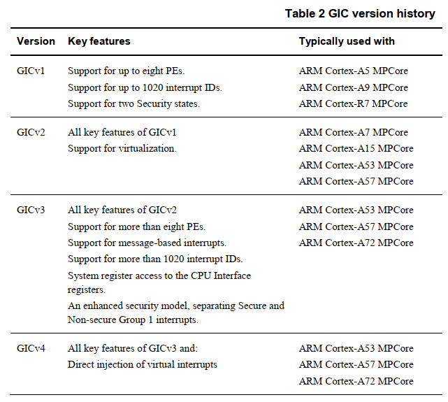
GICv1 and GICv2 support a maximum of eight PEs, which are insufficient. Therefore, GICv3 proposes the Affinity Routing mechanism to support more PEs.
GICv3 defines the following interrupt types (see Reference 6). Interrupt types on ARM:
- Locality-specific Peripheral Interrupt (LPI): LPIs are message-based, edge-triggered, and ITS-routed. Their configurations are stored in tables instead of registers. Typical LPIs include PCIe MSI/MSI-x interrupts and GITS_TRANSLATER control interrupts.
- Software Generated Interrupt (SGI): SGIs are interrupts triggered by software. Software can trigger an interrupt event by writing to the GICD_SGIR register. This interrupt is generally used for inter-core communication (corresponding to the x86 inter-processor interrupt).
- Private Peripheral Interrupt (PPI): A PPI is a private interrupt of each core. If a PPI is too long, it is sent to the specified CPU. A PPI is edge-triggered or electrical level-triggered and has the active state. Its application scenario is the CPU local clock. The PPI is similar to the LAPIC timer interrupt on x86.
- Shared Peripheral Interrupt (SPI): SPIs are edge-triggered or electrical level-triggered and have the active state. SPIs can be processed by multiple CPU cores, instead of a specified CPU. SPIs support the Message format (GICv3), GICD_SETSPI_NSR (for setting the interrupts), and GICD_CLRSPI_NSR (for clearing the interrupts).
Interrupts on ARM can also be classified into the following two types: One type is interrupts that are distributed by the distributor, such as SPIs. The other type is not distributed by the distributor, such as LPIs. Such interrupts are directly translated by the Interrupt Translation Service (ITS) and then sent to the redistributor.
| INTID | Interrupt Type | Notes |
|---|---|---|
| 0-15 | SGI | Banked per PE |
| 16-31 | PPI | Banked per PE |
| 32-1019 | SPI | |
| 1020-1023 | Special Interrupt Number | Used to signal special cases |
| 1024-8191 | Reserved | |
| 8192- | LPI |
GICv3 uses the Affinity Routing mechanism to identify a specific PE or a group of PEs. It is similar to the APICID/X2APIC ID mechanism on x86. ARM uses four 8-bit fields to indicate affinity. The format is as follows:
<affinity level 3>.<affinity level 2>.<affinity level 1>.<affinity level 0>For example, there is a mobile processor (SoC) in the ARM Big.Little architecture. The SoC has two clusters, four Cortex-A53 cores, and two A72 cores. The affinity can be set as follows:
0.0.0.[0:3] Cores 0 to 3 of a Cortex-A53 processor
0.0.1.[0:1] Cores 0 to 1 of a Cortex-A72 processor
The design of GICv3 is different from that of x86 IOAPIC/LAPIC. The following figure shows the architecture of GICv3.
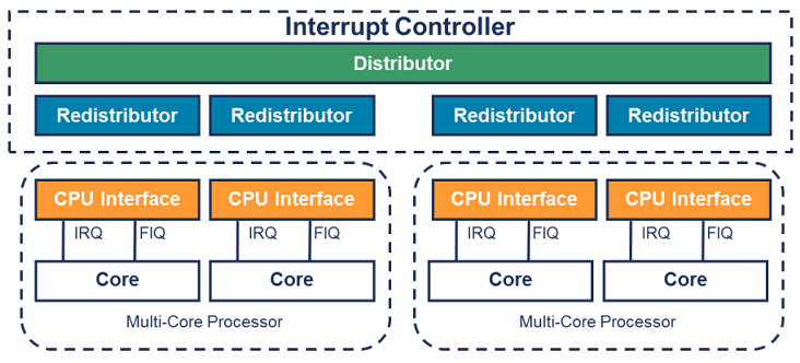
The GICv3 interrupt controller consists of the distributor, redistributor, and CPU interface. The distributor manages SPIs and sends SPIs to the redistributor. The redistributor manages PPIs, SGIs, and LPIs and sends them to the CPU interface. The CPU interface injects the interrupts into the core (the CPU interface is inside the core).
The distributor provides the following functions:
- Managing interrupt priorities and distributing interrupts
- Enabling and disabling SPIs
- Setting the interrupt priority for each SPI
- Setting routing information for each SPI
- Setting the interrupt triggering attribute (edge-triggered or electrical level-triggered) for each SPI
- Generating SPIs in message format
- Controlling the active and pending states of SPIs
Each PE is connected to a redistributor. The register of the distributor is memory-mapped, and its configuration takes effect globally and directly affects all PEs. The redistributor provides the following functions:
- Enabling and disabling SGIs and PPIs
- Setting the priorities of SGIs and PPIs
- Setting the PPI triggering attribute (electrical level-triggered or edge-triggered)
- Allocating each SGI and PPI to an interrupt group
- Controlling the SGI and PPI state
- Controlling base addresses of data structures related to LPIs
- Supporting PE power management
Each redistributor is connected to a CPU interface. In GICv3, the register of the CPU interface is accessed through system registers (ICC_*ELn). Before using these registers, the system registers must be enabled. The main functions of the CPU interface are as follows:
- Controlling CPU interrupt handling. If an interrupt is disabled, even if the distributor distributes an interrupt event to the CPU interface, the interrupt event is masked by the core.
- Answering to interrupts
- Detecting interrupt priorities and de-asserting interrupts
- Setting an interrupt priority mask flag for a PE to mask interrupts
- Defining a preemption policy for a PE
- Determining the highest priority of the current pending interrupt for a PE (priority arbitration)
GICv3 introduces the ITS component to process LPIs. When a peripheral need to send an LPI, it writes data to the ITS register GITS_TRANSLATER. This write operation triggers an LPI. After receiving the LPI, the ITS parses the interrupt and sends it to the corresponding redistributor. Then, the redistributor sends the interrupt to the CPU interface. What are the contents included in the write operation? There are two key fields.
- EventID: value written to GITS_TRANSLATER. The event ID defines the ID of the interrupt to be triggered by the peripheral. It can be the same as the interrupt ID (INTID) or an INTID obtained after ITS translation.
- DeviceID: device (peripheral) ID. The implementation is user-defined. For example, the AXI user signal can be used to transfer it.
The ITS uses three types of tables to translate and route LPIs:
- Device table: maps the device ID to the interrupt translation table.
- Interrupt translation table: contains the mapping between the event ID and INTID, device ID information, and INTID collections.
- Collection table: maps collections to the redistributor.
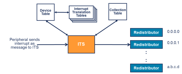
The entire process is as follows:
Step 1: The peripheral writes data to GITS_TRANSLATER. The ITS uses the device ID to find the interrupt translation table to be used by the peripheral from the device table.
Step 2: The ITS uses the event ID to select the INTID and the corresponding collection ID from the interrupt translation table.
Step 3: The ITS uses the collection ID to select the corresponding collection and route information from the collection table.
Step 4: The ITS sends the interrupt to the target redistributor.
The preceding only introduces the logic of the GICv3 interrupt controller. For details about how to implement it in QEMU/KVM, you can refer to the corresponding code. To improve the interrupt performance, GICv3 simulation is implemented in KVM. For example, the MSI interrupt of a virtio device is an LPI interrupt. During QEMU simulation, the irqfd mechanism is used. Later, I will analyze the implementation from the perspective of code.
5. Summary
The ARM architecture is different from the x86 architecture. The biggest difference is the interrupt controller. Memory virtualization and I/O virtualization may be different in detail, but their principles are similar. For example, both the SMMUv3 and Intel IOMMU support two-stage address translation in design, but the SMMU has targeted improvements. For more information about ARM virtualization, see the ARMv8 specifications documentation.


